1. はじめに
1.1 研究前提と市場定義
1.2 研究範囲
2. 研究方法論
3. エグゼクティブサマリー
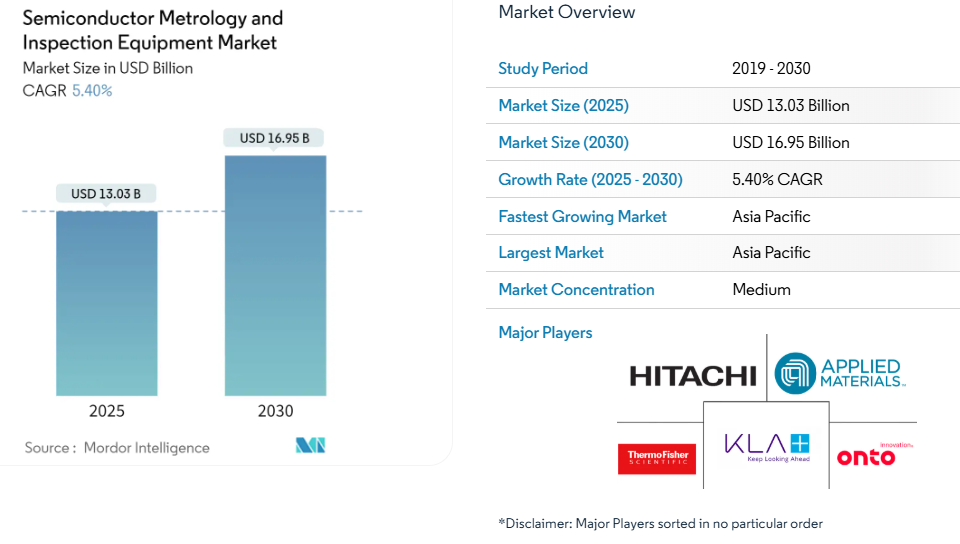
4. 市場概況
4.1 市場概要
4.2 市場推進要因
4.2.1 7 nm ノード以下の精度に対する需要の高まり
4.2.2 3D NAND および先進メモリ生産の成長
4.2.3 APAC におけるファウンドリ生産能力の拡大
4.2.4 ハイブリッドボンディング計測技術の採用
4.2.5 ツールのダウンタイムを削減する現場での AI 分析
4.2.6 低欠陥歩留まりを推進する持続可能性の義務
4.3 市場の制約
4.3.1 電子ビームおよび EUV ツールの高額な設備投資
4.3.2 熟練した計測エンジニアの不足
4.3.3 ヘリウムおよび特殊ガスのサプライチェーンのリスク
4.3.4 クラウドベースの検査におけるデータセキュリティの懸念
4.4 業界のバリューチェーン分析
4.5 規制の展望
4.6 技術の見通し
4.7 ポーターの5つの力分析
4.7.1 供給者の交渉力
4.7.2 購入者の交渉力
4.7.3 新規参入の脅威
4.7.4 代替品の脅威
4.7.5 競争の激しさ
4.8 マクロ経済要因が市場に与える影響
5. 市場規模と成長予測 (金額ベース)
5.1 測定タイプ別
5.1.1 リソグラフィ計測
5.1.1.1 オーバーレイ
5.1.1.2 寸法測定装置
5.1.1.3 マスク検査・計測
5.1.2 ウェーハ検査
5.1.3 薄膜計測
5.1.4 その他のプロセス制御システム
5.2 技術ノード別
5.2.1 3nm未満
5.2.2 3nm
5.2.3 5nm
5.2.4 7nm
5.2.5 14/16nm
5.2.6 28nm
5.2.7 28nm超
5.3 半導体デバイスタイプ別
5.3.1 ロジックIC
5.3.2 メモリIC
5.3.3 アナログおよびミックスドシグナルIC
5.3.4 パワーデバイス
5.3.5 オプトエレクトロニクス
5.4 最終用途産業別
5.4.1 民生用電子機器
5.4.2 コンピューティングおよびデータセンター
5.4.3 自動車・輸送機器
5.4.4 産業用機器
5.4.5 医療・ライフサイエンス
5.4.6 航空宇宙・防衛
5.4.7 その他のエンドユーザー産業
5.5 地域別
5.5.1 北米
5.5.1.1 アメリカ合衆国
5.5.1.2 カナダ
5.5.1.3 メキシコ
5.5.2 欧州
5.5.2.1 ドイツ
5.5.2.2 イギリス
5.5.2.3 フランス
5.5.2.4 イタリア
5.5.2.5 その他の欧州
5.5.3 アジア太平洋地域
5.5.3.1 中国
5.5.3.2 日本
5.5.3.3 韓国
5.5.3.4 インド
5.5.3.5 アジア太平洋その他
5.5.4 南アメリカ
5.5.4.1 ブラジル
5.5.4.2 アルゼンチン
5.5.4.3 南アメリカその他
5.5.5 中東・アフリカ
5.5.5.1 中東
5.5.5.1.1 アラブ首長国連邦
5.5.5.1.2 サウジアラビア
5.5.5.1.3 トルコ
5.5.5.1.4 中東その他
5.5.5.2 アフリカ
5.5.5.2.1 南アフリカ
5.5.5.2.2 ケニア
5.5.5.2.3 ナイジェリア
5.5.5.2.4 アフリカその他
6. 競争環境
6.1 市場集中度
6.2 戦略的動向
6.3 ベンダー市場シェア分析
6.4 企業プロファイル(グローバル概要、市場レベル概要、中核セグメント、入手可能な財務情報、戦略情報、主要企業の市場順位/シェア、製品・サービス、最近の動向を含む)
6.4.1 ASML Holding N.V.
6.4.2 KLA Corporation
6.4.3 Applied Materials, Inc.
6.4.4 Onto Innovation Inc
6.4.5 日立ハイテク株式会社
6.4.6 Thermo Fisher Scientific Inc
6.4.7 浜松ホトニクス株式会社
6.4.8 Nova Measuring Instruments Ltd.
6.4.9 レーザーテック株式会社
6.4.10 Camtek Ltd.
6.4.11 日本電子株式会社
6.4.12 株式会社ニコン
6.4.13 東京エレクトロン株式会社
6.4.14 スクリーン半導体ソリューションズ株式会社
6.4.15 株式会社アドバンテスト
6.4.16 カールツァイスAG
6.4.17 メルクKGaA
6.4.18 東レエンジニアリング株式会社
6.4.19 マイクロトロニック株式会社
6.4.20 ブルカー株式会社
6.4.21 ノードソン株式会社
6.4.22 コンフォビス社
6.4.23 コメット・イクソン社(コメット・ホールディングAG)
7. 市場機会と将来展望
7.1 ホワイトスペースと未充足ニーズの評価
ーーーーーーーーーーーーーーーーーーーーーーーーーーーーーーーーーーーーーー
1. INTRODUCTION
1.1 Study Assumptions and Market Definition
1.2 Scope of the Study
2. RESEARCH METHODOLOGY
3. EXECUTIVE SUMMARY
4. MARKET LANDSCAPE
4.1 Market Overview
4.2 Market Drivers
4.2.1 Rising Demand for Sub-7 nm Node Accuracy
4.2.2 Growth in 3D NAND and Advanced Memory Production
4.2.3 Expansion of Foundry Capacities in APAC
4.2.4 Adoption of Hybrid Bonding Metrology
4.2.5 In-situ AI Analytics Reducing Tool Downtime
4.2.6 Sustainability Mandates Driving Low-Defect Yields
4.3 Market Restraints
4.3.1 High Capital Expenditure of E-beam and EUV Tools
4.3.2 Shortage of Skilled Metrology Engineers
4.3.3 Supply Chain Risks for Helium and Specialty Gases
4.3.4 Data-Security Concerns in Cloud-Based Inspection
4.4 Industry Value Chain Analysis
4.5 Regulatory Landscape
4.6 Technological Outlook
4.7 Porter’s Five Forces Analysis
4.7.1 Bargaining Power of Suppliers
4.7.2 Bargaining Power of Buyers
4.7.3 Threat of New Entrants
4.7.4 Threat of Substitutes
4.7.5 Degree of Competition
4.8 Impact of Macroeconomic Factors on the Market
5. MARKET SIZE AND GROWTH FORECASTS (VALUE)
5.1 By Measurement Type
5.1.1 Lithography Metrology
5.1.1.1 Overlay
5.1.1.2 Dimension Equipment
5.1.1.3 Mask Inspection and Metrology
5.1.2 Wafer Inspection
5.1.3 Thin Film Metrology
5.1.4 Other Process Control Systems
5.2 By Technology Node
5.2.1 Less Than 3 nm
5.2.2 3 nm
5.2.3 5 nm
5.2.4 7 nm
5.2.5 14/16 nm
5.2.6 28 nm
5.2.7 Greater Than 28 nm
5.3 By Semiconductor Device Type
5.3.1 Logic IC
5.3.2 Memory IC
5.3.3 Analog and Mixed Signal IC
5.3.4 Power Devices
5.3.5 Optoelectronics
5.4 By End-Use Industry
5.4.1 Consumer Electronics
5.4.2 Computing and Data Centers
5.4.3 Automotive and Transportation
5.4.4 Industrial
5.4.5 Healthcare and Life Sciences
5.4.6 Aerospace and Defense
5.4.7 Other End User Industries
5.5 By Geography
5.5.1 North America
5.5.1.1 United States
5.5.1.2 Canada
5.5.1.3 Mexico
5.5.2 Europe
5.5.2.1 Germany
5.5.2.2 United Kingdom
5.5.2.3 France
5.5.2.4 Italy
5.5.2.5 Rest of Europe
5.5.3 Asia-Pacific
5.5.3.1 China
5.5.3.2 Japan
5.5.3.3 South Korea
5.5.3.4 India
5.5.3.5 Rest of Asia-Pacific
5.5.4 South America
5.5.4.1 Brazil
5.5.4.2 Argentina
5.5.4.3 Rest of South America
5.5.5 Middle East and Africa
5.5.5.1 Middle East
5.5.5.1.1 United Arab Emirates
5.5.5.1.2 Saudi Arabia
5.5.5.1.3 Turkey
5.5.5.1.4 Rest of Middle East
5.5.5.2 Africa
5.5.5.2.1 South Africa
5.5.5.2.2 Kenya
5.5.5.2.3 Nigeria
5.5.5.2.4 Rest of Africa
6. COMPETITIVE LANDSCAPE
6.1 Market Concentration
6.2 Strategic Moves
6.3 Vendor Market Share Analysis
6.4 Company Profiles (includes Global level Overview, Market level overview, Core Segments, Financials as available, Strategic Information, Market Rank/Share for key companies, Products and Services, and Recent Developments)
6.4.1 ASML Holding N.V.
6.4.2 KLA Corporation
6.4.3 Applied Materials, Inc.
6.4.4 Onto Innovation Inc
6.4.5 Hitachi High-Tech Corporation
6.4.6 Thermo Fisher Scientific Inc
6.4.7 Hamamatsu Photonics K.K.
6.4.8 Nova Measuring Instruments Ltd.
6.4.9 Lasertec Corporation
6.4.10 Camtek Ltd.
6.4.11 JEOL Ltd.
6.4.12 Nikon Corporation
6.4.13 Tokyo Electron Limited
6.4.14 SCREEN Semiconductor Solutions Co., Ltd.
6.4.15 Advantest Corporation
6.4.16 Carl Zeiss AG
6.4.17 Merck KGaA
6.4.18 Toray Engineering Co., Ltd.
6.4.19 Microtronic, Inc.
6.4.20 Bruker Corporation
6.4.21 Nordson Corporation
6.4.22 Confovis GmbH
6.4.23 Comet Yxlon GmbH (Comet Holding AG)
7. MARKET OPPORTUNITIES AND FUTURE OUTLOOK
7.1 White-space and Unmet-need Assessment


